
官方授權台灣代理分銷
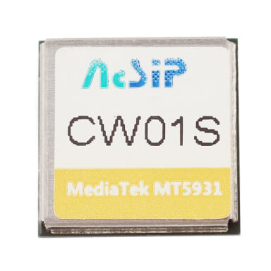
LinkIt MT2502A 模組-大規模解決方案

原名
LinkIt MT2502A Module -Scale for IoT solution
貨號
317030022
分類
Kits
特價
1,314
商品停售
由於停止生產、銷量不佳、升級改版... 或其他因素,SeeedStudio 原廠目前已經停止生產、供應、或銷售本件商品,請尋找其他替代品方案。
資料來源:https://www.seeedstudio.com/LinkIt-MT2502A-Module--Scale-for-IoT-solution-p-2399.html
Description
LinkIt MT2502A Module is a low-cost and low-power consumption IoT SiP module. The module is an operating deisgned for Wearables and Internet of Things(IoT)devices that can connect to other smart devices or directly to cloud applications and services. It integrates voice-band,audio-band,base-band analog front-end and full-featured power management unit. With its embedded support for GPRS/GSM, this highly integrated SoC design avoids the need for multiple chips, meaning smaller devices and reduced costs for device creators, as well as eliminating the need for compatibility tests. This module is complemented by Wi-Fi and GNSS chips, offering high performance and low power consumption to devices with more sophisticated communication or location acquisition requirements.With LinkIt MT2502A Module, it’s easier and cheaper for device manufacturers to produce desirable, functional wearable products.
Features:
General
Integrated voice-band, audio-band and base-band analog front-end
Integrated full-featured power management unit
MCU subsystem
ARM7EJ-S TM 32-bit RISC processor
Java hardware acceleration for fast Java-based games and applets
High-performance multi-layer AHB bus
Dedicated DMA bus with 16 DMA channels
On-chip boot ROM for factory flash programming
Watchdog timer for system crash recovery
3 sets of general-purpose timers
Circuit switch data coprocessor
Division coprocessor
Serial flash interfaces
Supports various operating frequency combinations for serial flash
Supports QPI and SPI serial flash
User interfaces
5-row x 5-column keypad controller with hardware scanner
Supports multiple key presses for gaming
Dual SIM/USIM controller with hardware T=0/T=1 protocol control
Real-time clock(RTC) operating with a low-quiescent-current power supply
General-purpose I/Os(GPIOs) available for auxiliary applications
2 sets of Pulse Width Modulation(PWM) output
24 external interrupt lines
1 external channel auxiliary 10-bit A/D converter
Security
Supports security key and chip random ID
Connectivity
3 UARTs with hardware flow control and supports baud rate up to 921600bps
FS/LS USB 1.1 device controller
Multimedia card, secure digital Memoy Card, host controller with flexible I/O voltage power
Supports 4-bit SDIO interface for SDIO peripherals as well as WIFI connectivity
DAI/PCM and I2S interface for audio applications
I2C master interface for peripheral management including image sensors
SPI master/slave interface for peripheral management.
Power management
Li-ion battery charger
12 LDOs for the power supply of memory card, camera, Bluetooth, RF, SIM card and other diversified usage.
1 open-drain output switches to supply/control the LED
LDO type vibrator
One NMOS switch to control keypad LED
Thermal overload protection
Under-voltage protection
Different levels of power-down modes with sophisticated software control enables excellent power saving performance
Test and debugging
Built-in digital and analog loop back modes for both audio and baseband front-end
DAI port complies with GSM Rec.11.10
JTAG port for debugging embedded MCU
Specification:
Model Name: AI2502S05
Chipset: MT2502A
Core: ARM7 EJ-STM
Clock Speed: 260MHz
Flash: 16MB
RAM: 4MB
Operation Conditions
Temperature: -20℃~70℃(Operating),-40℃~85℃(Storage)
Humidity:10~95%(Operating),5~95%(Storage)
Dimension:17mm x 15mm x 1.8mm(Max.)
Package:LGA
Electrical Specifications
Digital IO Pins:TBD(Pin Count),3.3V(Voltage)
Analog Input Pins:TBD(Pin Count),0~5V(Voltage)
PWM Output Pins: Max Resolution:13bit
Max Frequency@Resolution:
1.6kHz@13bit
50.8KHz@8bit
800kHz@4bit
I2C(master only): 100Kbps, 400Kbps, 3.4Mbps
SPI (master only): 104Kbps~26Mbps
GSM/GPRS: 850/900/1800/1900 MHz
Bluetooth: BR/EDR/BLE(Dual Mode)
Technical Details
| Weight | G.W 0g |
| Battery | Exclude |
描述
LinkIt MT2502A 模組是一種低成本、低功耗的 SiP 模組。該模組是一個操作 deisgned 的 "和互聯網的東西 (物) 設備, 可以連接到其他智慧設備或直接到雲應用程式和服務。它集成了語音波段、音訊波段、基帶類比前端和全功能電源管理單元。通過對 GPRS/GSM 的嵌入式支援, 這種高度集成的 SoC 設計避免了對多個晶片的需求, 意味著設備建立者的小設備和成本降低, 同時也消除了對相容性測試的需求。該模組輔以 wi-fi 和 GNSS 晶片, 提供高性能和低功耗的設備, 具有更複雜的通信或位置獲取要求。使用 LinkIt MT2502A 模組, 設備製造商可以更方便、更便宜地生產出理想的、功能齊全的耐磨產品。
功能:
秘書長
集成語音波段、音訊波段和基帶類比前端
集成式全功能電源管理單元
單片機子系統
ARM7EJ-S TM 32 位 RISC 處理器
java 硬體加速, 用於快速基於 java 的遊戲和 applet
高性能多層 AHB 匯流排
具有 16 dma 通道的專用 dma 匯流排
用於工廠 flash 程式設計的片上引導 ROM
系統崩潰恢復的看門狗計時器
3套通用計時器
電路開關資料副處理器
除法副處理器
串列快閃記憶體介面
支援串列快閃記憶體的各種工作頻率組合
支援 QPI 和 SPI 串列快閃記憶體
使用者介面
帶硬體掃描器的5行 x 5 列小鍵盤控制器
支援多按鍵遊戲
具有硬體 T=0/T=1 協定控制的雙 SIM/USIM 控制器
使用低靜態電流電源的系統時鐘 (RTC)
適用于輔助應用程式的通用 i/o (個)
2套脈寬調製 (PWM) 輸出
24外部中斷線路
1外部通道輔助10位 a/d 轉換器
安全
支援安全金鑰和晶片隨機 ID
連接
3 uart, 硬體流量控制, 支援串列傳輸速率高達921600bps
FS/LS USB 1.1 設備控制器
多媒體卡、安全數位 Memoy 卡、具有靈活 i/o 電壓的主機控制器
支援 SDIO 週邊設備的4位 SDIO 介面以及 WIFI 連接
音訊應用的 DAI/PCM 和 I2S 介面
I2C 包括圖像感應器在內的週邊管理的主介面
用於週邊管理的 SPI 主/從屬介面。
電源管理
鋰離子電池充電器
12穩壓用於儲存卡、攝像頭、藍牙、射頻、SIM 卡等多種用途的電源。
1開路輸出開關提供/控制 LED
LDO 型振動器
一個 NMOS 開關控制鍵盤 LED
熱超載保護
低壓保護
不同級別的斷電模式與先進的軟體控制, 使優秀的節電性能
測試和調試
內置數位和類比環路的音訊和基帶前端模式
戴港符合 GSM Rec 11.10
用於調試嵌入式 MCU 的 JTAG 埠
規範:
型號名稱: AI2502S05
晶片組: MT2502A
核心: ARM7 EJ-STM
時脈速度: 260MHz
閃光燈: 16MB
RAM: 4MB
操作條件
溫度:-20℃〜 70℃ (操作),-40℃〜 85℃ (存儲)
濕度:10 ~ 95% (操作), 5 ~ 95% (存儲)
dimension:17mm x 15mm x 1.5~1.8mm (最大)
包裝: 伊賀
電氣規格
數位 IO 針腳: 待定 (Pin 計數), +3.3v (電壓)
類比輸入引腳: 待定 (Pin 計數), 0 ~ 5 v (電壓)
PWM 輸出引腳: 最大 resolution:13bit
最大 Frequency@Resolution:
1.6kHz@13bit
50.8KHz@8bit
800kHz@4bit
I2C (僅限主): 100Kbps、400Kbps、3.4Mbps
SPI (僅限主控): 104 kbps ~ 26 mbps
GSM/GPRS: 850/900/1800/1900 MHz
藍牙: BR/EDR/雙模
技術細節
| 重量 | G. W 0g |
| 電池 | 排除 |